Forward biased p-n junction diode What is forward bias and reverse bias? example, applications Diode biased pn biasing bias definition electricalworkbook
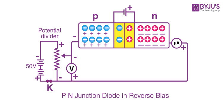
Reverse Biasing of PN Junction Diode - Definition, Theory & Diagram
Diode junction pn bias forward characteristics depletion voltage electronics current region circuits mosfet bjt formation biased reverse semiconductors under ws
Pn junction diode forward bias current part 1
Junction bias draw arrangement studying pn diode reverse plot reversed obtainingPn junction diode forward and reverse bias Forward junction diode biasingPn junction diode: forward and reverse bias characteristics.
Pn junction forward bias circuit diagramMiirbe pn junction diode forward bias diagram P-n junctionElectrical – how to discharge the pn junction capacitance – valuable.
Diode pn semiconductor junction layer depletion working bias reverse characteristics notes physics flow circuit electronics biasing type battery choose board
Reverse biasing of pn junction diodeForward biasing of p-n junction diode Pn junction diode and its forward bias & reverse bias characteristicsPn junction diode.
Diode actionSemiconductor diode Forward and reverse bias of a pn junction (explained)Diode forward junction bias types pn working electrical4u reverse biased diodes principle current diffusion under type symbol semiconductor electrons depletion.

Forward and reverse bias circuit diagram
What is a junction diode? what are the types of junction diodesBias reverse forward diode electronics Draw the circuit arrangement for studying v-i characteristics of a p-nDiode forward bias circuit diagram.
Bias diode forward pn junction currentForward diode junction biased hole current semiconductor electron diodes bias holes voltage applied Biasing difference bias diode voltageDiodo a giunzione pn e caratteristiche del diodo.

Forward biasing of pn junction diode
To draw the i-v characteristic curve of a p-n junction in forward biasForward bias and reverse bias of pn junction diode ☑ diode zero biasSemiconductor diode.
Junction forward region depletion diagram pn biased showing including figurePn junction circuit diagram zero bias Diode junction pn forward bias characteristics circuit biasing reverse ammeter voltmeter plot sourcePn junction diode animation ppt.

Schematic diagram of forward biased diode
Junction diode forward biasing working bias pn its reverse voltage introductionPn junction diode (forward-bias condition), 58% off Diode pn zener bias chart pptBias biasing pn diode junction etechnog transistors barrier.
An introduction to p-n junction diode and its workingBias pn junction diode Pn junction under reverse bias condition☑ diode zero bias.


